The Diode Clock
April 2025 - January 2026


The Diode Clock is a 24-hour clock built to test diode logic, a unique new universal digital logic family. The clock was designed by Ted Yapo from 2012 to 2016, and he documented the project on Hackaday. I remade Yapo's clock with additions and redesigns.In diode logic, a 1N4007 diode forms an inverter by switching radio-frequency (RF) current based on logic-level signals. Combined with a 1N4148-based OR gate, a NOR gate is formed, from which any combinational or sequential logic function can be created.The clock contains RF power supplies, diode logic gates, diode encoders, a spectrum generator, diode displays, display amplifiers, and a crystal oscillator timebase. The power supplies, spectrum generator, display amplifiers, and timebase required transistors and ICs. 62 PCBs distribute 6000+ total components.As transistor scaling slows, alternative computing methods become more important. Diode logic won’t replace transistor-based TTL or CMOS. But I’ve had fun and learned a lot exploring its quirks.
30 Hz operation
1. Diode Clock Logic Board
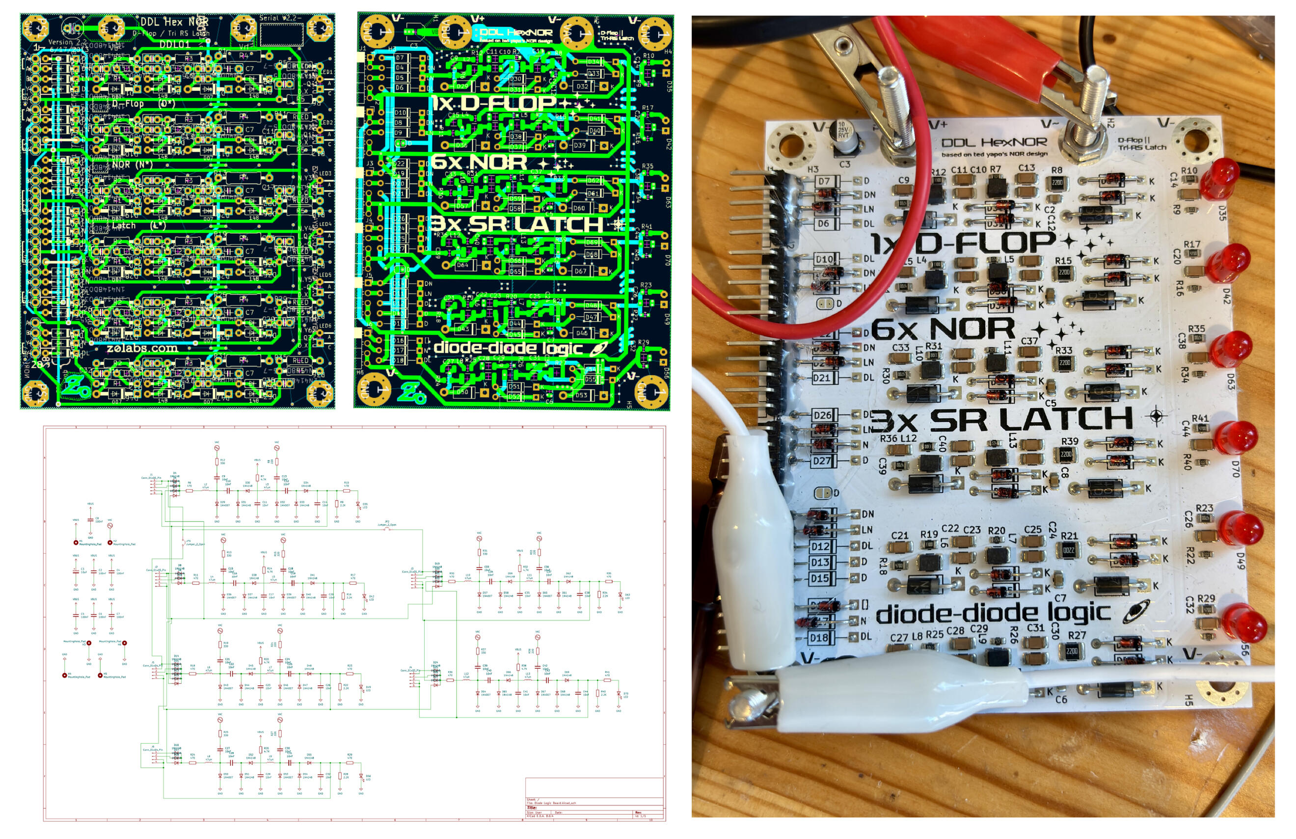
After building TenniBear, I wanted to work on something purely electronic. While browsing Hackaday, I found Ted Yapo’s Diode Clock. The clock stood out to me for the wide range of electronics involved and the complexity. I predicted building the clock would keep me occupied for months and teach me more about electrical engineering. After a few days of poring over Yapo's project logs, I committed to building his clock with some redesigns.The clock is built around logic boards. The top left is design is his. To the right is mine, with fewer through-hole components and thicker traces. Manual assembly/soldering time was reduced from around 1 hour/board (for Yapo’s design) to 15 minutes. Using JLCPCB instead of OSH Park (Yapo's supplier) reduced prices from $20/board to $4/board.The board consists of six NOR gates each made of diodes, capacitors, resistors, and inductors. The board is reconfigurable as a data flip flop or 3 set-reset latches. The red LEDs display output state. Powered with 5V DC and 12Vp-p RF supplied by custom power supply (next slide).
~Redesigned April 2025, finished assembly August
2. Diode Clock Radio-Frequency Power Supply Board
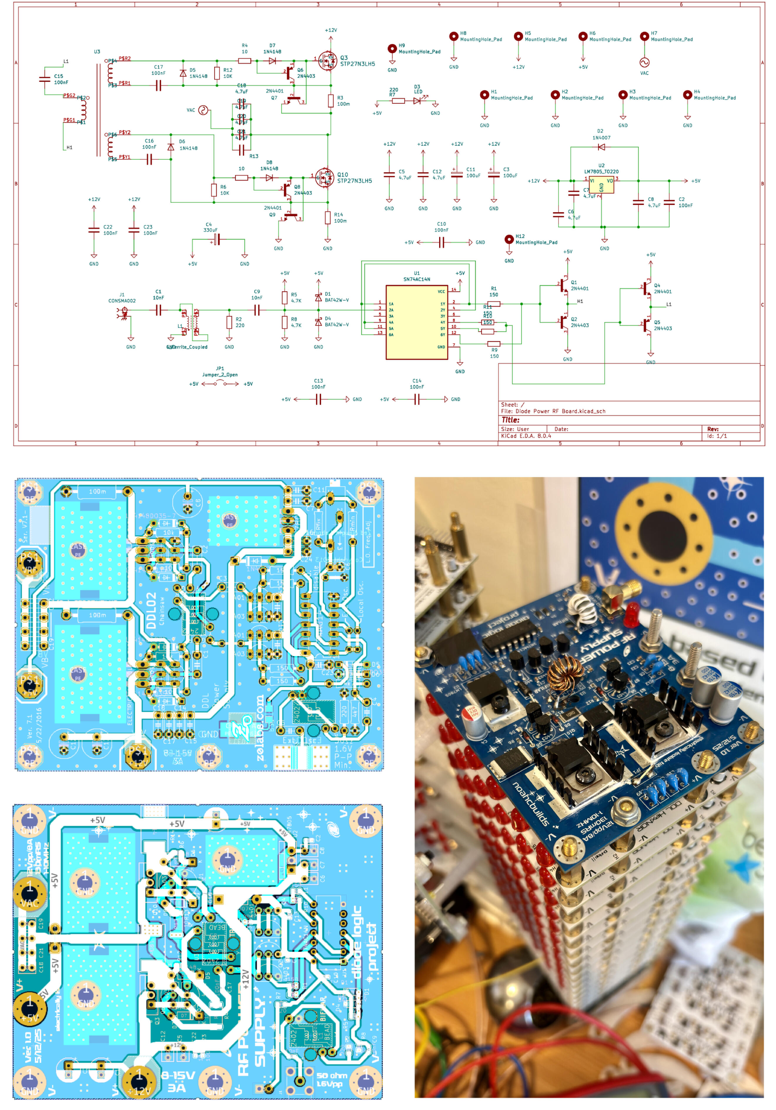
Yapo’s diode logic NOR gates require an RF power source (middle left), which allows for signal inversion (DC bias from inputs inversely determining whether RF current is shunted to ground via diodes, resulting in a low output, or blocked and allowed to continue, producing a high output). Bottom left is my redesign, with the local oscillator section removed. As with all the original boards, many components Yapo selected were no longer manufactured, so I found ones with similar ratings. I also increased the power rating of the current-limiting resistors (R3 and R14 in schematic).Assembly of the switching MOSFETs was delicate, with layers of insulation, thermal grease, and heatsinks. Bottom right is a picture of an assembled power supply on top of a stack of logic boards. Three of these “logic stacks” make up my version of the clock.
~Redesigned April 2025, finished assembly August
3. Diode Clock Divisor, Spread Spectrum Generator, 7-Segment Diode Encoder
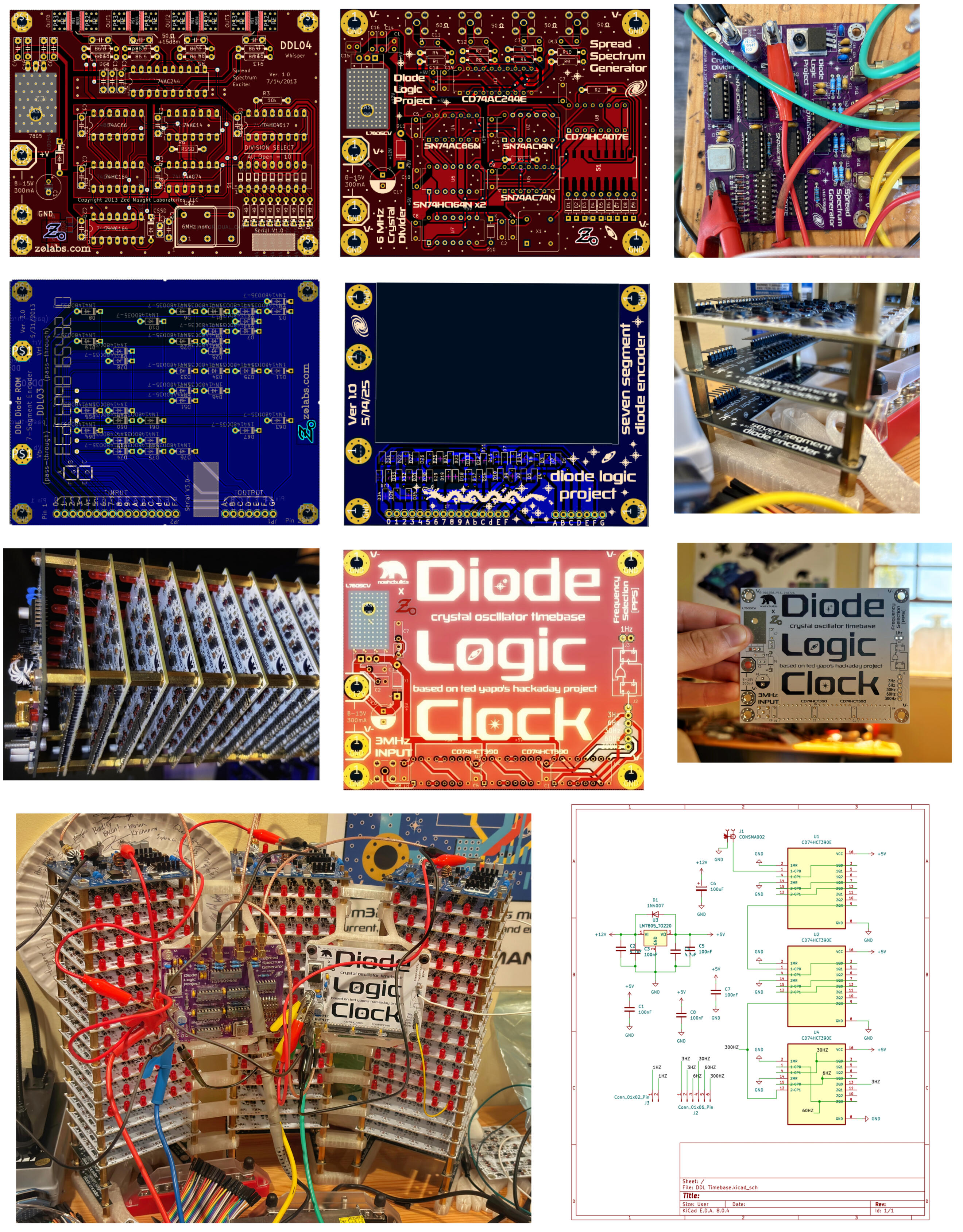
Top pictures depict the external oscillator used for the power supply input signals. I kept this board mostly identical to Yapo’s, except for some footprints (SMA jack, crystal). The board provides 3 MHz signals to 4 RF power supplies, reducing EMI by keeping them in opposite phases. I condensed my clock to 3 power supplies, which made the build process simpler but reduced the anti-EMI effectiveness.Below the spectrum generator is a diode encoder for 7-segment displays (the display boards I have yet to make). The bright red board is my self-designed timebase, dividing the 4th output of the spectrum generator (3 MHz) down to 1 Hz (clock source). I chained three 4-bit decade counter ICs in series to get from 3 MHz to 3 Hz. To get from 3 Hz to 1 Hz, I use two D flip flops and an extra NOR gate. Bottom right is the schematic of the timebase, and bottom left are my three “logic stacks” with the spectrum generator and timebase.
~Redesigned May 2025, finished assembly August
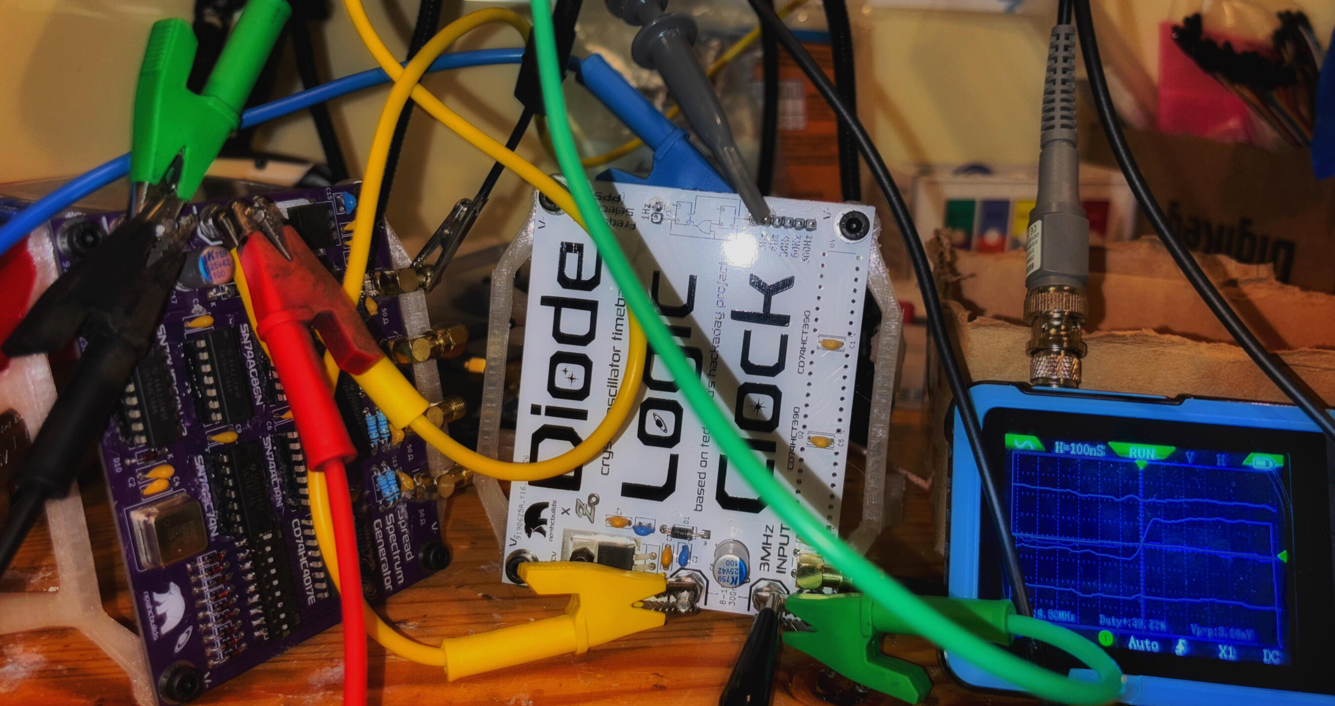
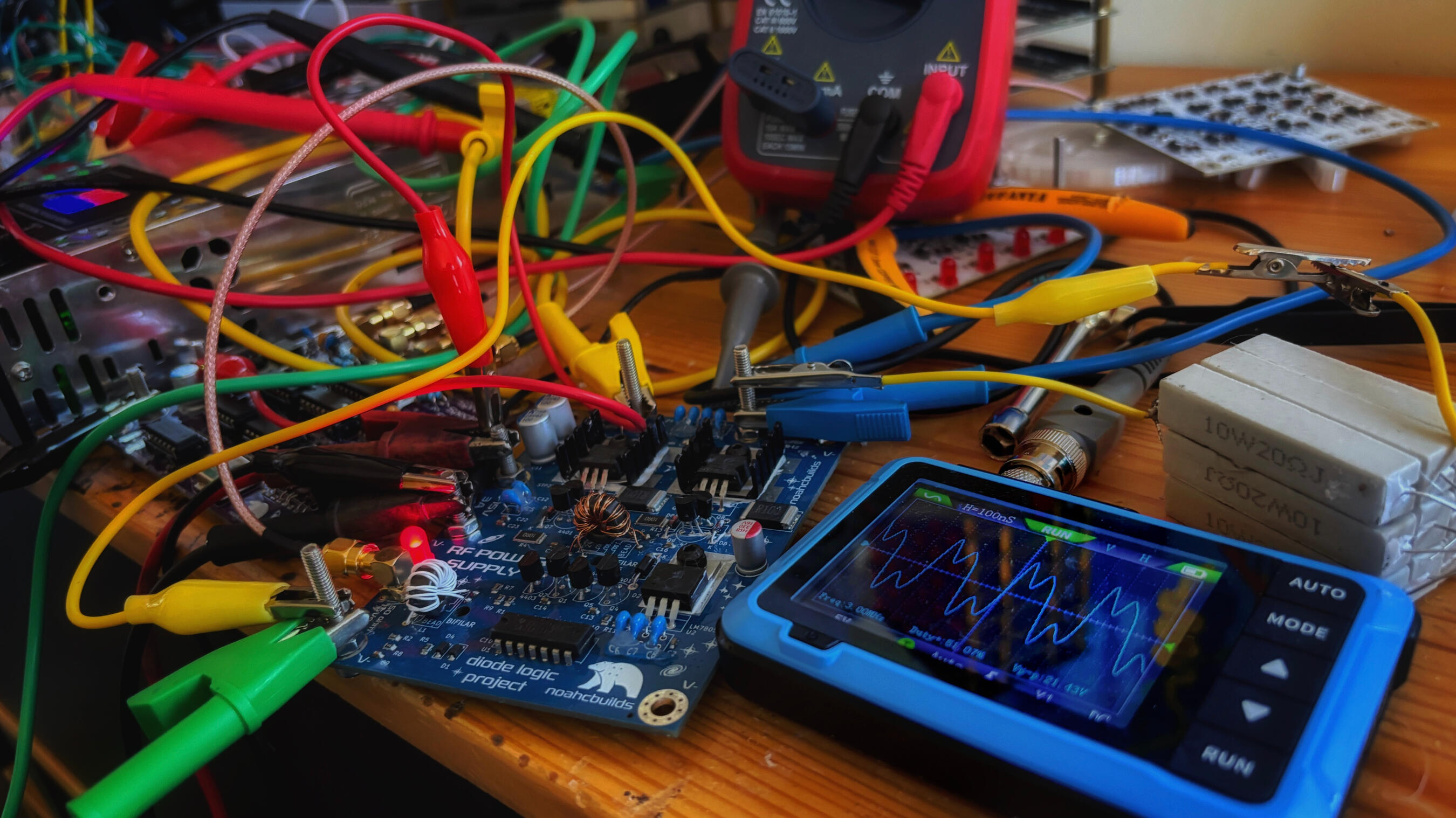
4. Diode Clock Power Supply + Logic Board Testing
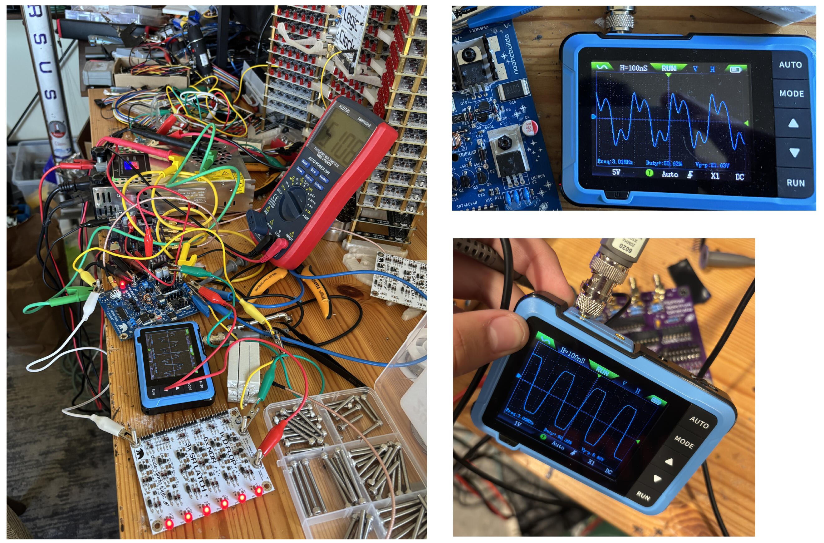
After finishing assembly of the signal generator and power supply, I needed to verify their performance. My school didn’t have an oscilloscope, so I bought a cheap handheld one off Amazon.Bottom right is the output of the signal generator, a clean 3 MHz 5.5Vp-p square wave. I fed this into the RF power supply, obtaining the upper right waveform with a 2.2 ohm dummy load (nine 20-ohm resistors in parallel, which I measured from my logic stack to be a good model of the load). The result contained 22V spikes and 12Vp-p averages. These spikes are within my MOSFETs’ 30V limit, although my oscilloscope’s 10 MHz sampling rate makes it hard to be sure. MOSFET temperature stabilized around 35C.
~August to September 2025
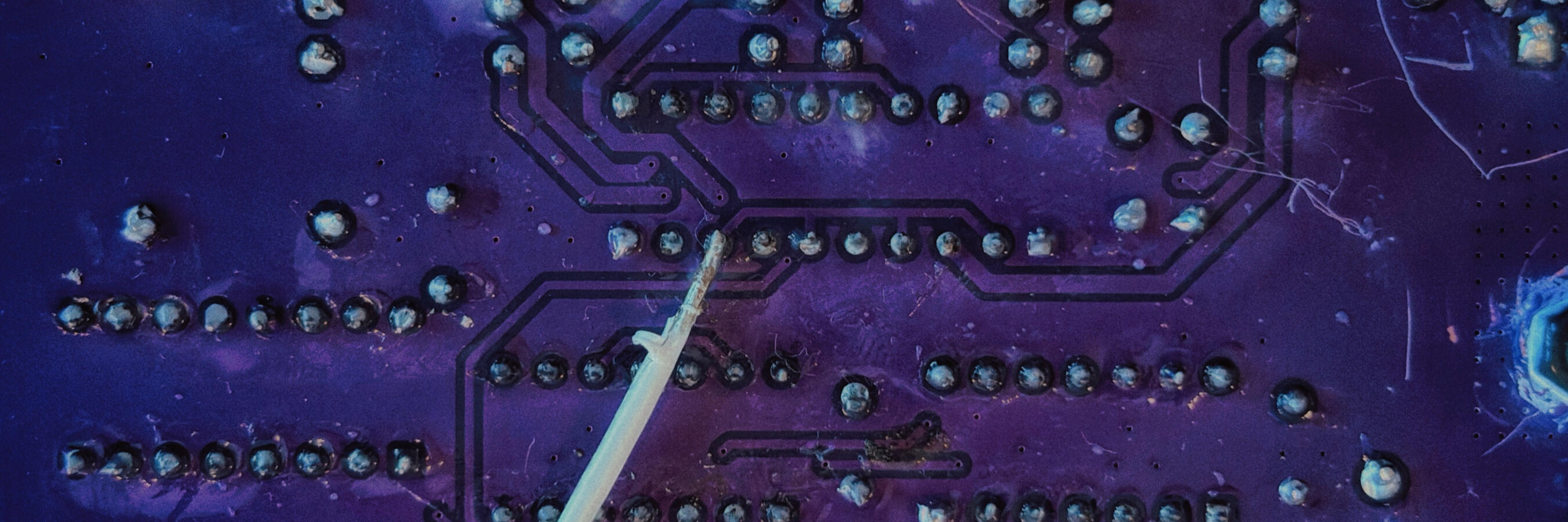
5. Diode Clock Logic Board Debugging
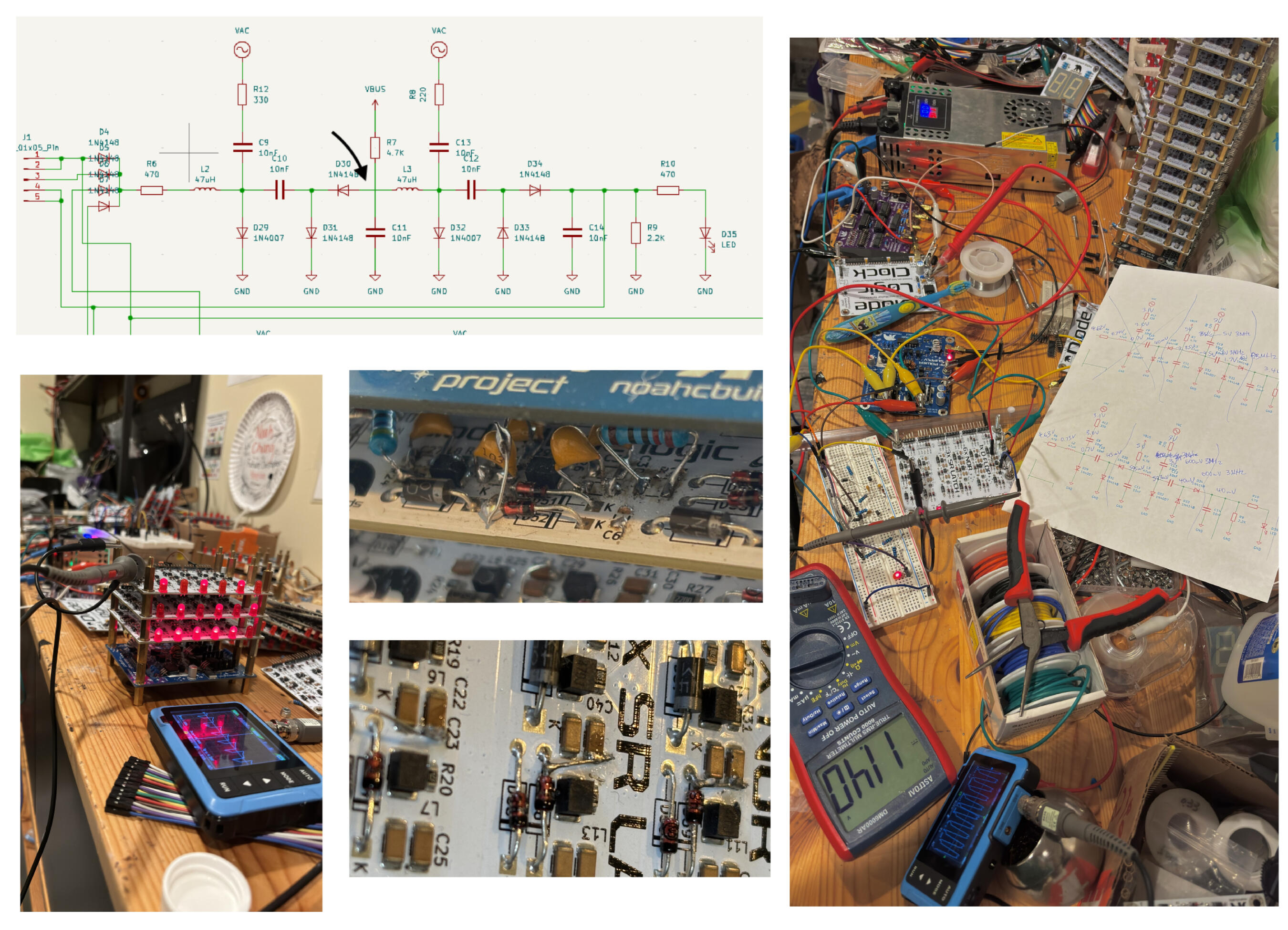
I didn't catch this while creating the logic board, but I'd missed a connection at the highlighted node (black arrow, top left). KiCad makes it hard to spot, especially if I don't zoom in all the way.I discovered the effects of this while testing the boards. After feeding signals to the NOR gates, the outputs would remain high. I breadboarded a single logic gate, which functioned properly, and compared the voltages at every node with those on the PCB (right). I noticed they started differing at the aforementioned node, but was unsure why. I swapped components back and forth between the breadboard and the PCB (center middle), eventually realizing that two components that should have been connected were not. I spent another few days fixing this by soldering external connections (bottom middle) to all 6 NOR gates of every logic board.The first logic board module I assembled and tested was the mod 3 counter (bottom left), which takes the 3 Hz from the output of my timebase down to 1 Hz for the clock source.
~September to January 2025
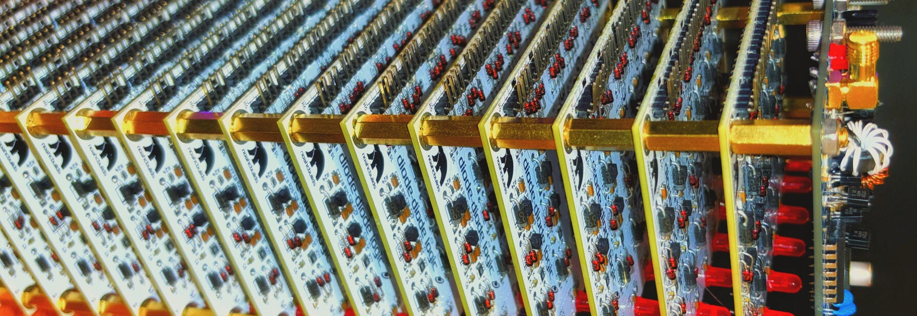
6. Diode Clock Logic Stack Assembly
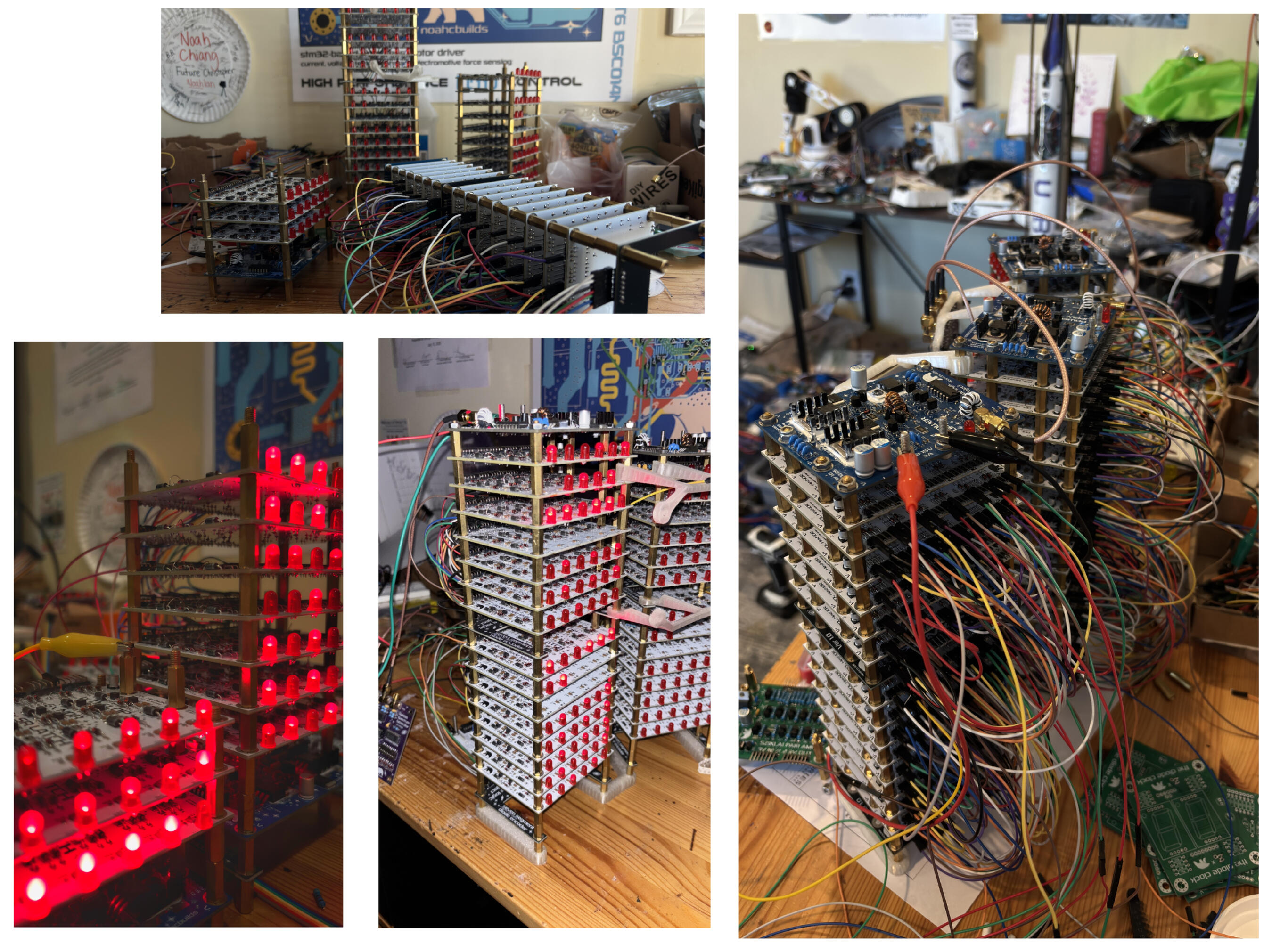
After the mod 3 counter was a mod 10/decade counter (the taller tower in the bottom left picture). The bottom five logic boards are configured as D flip-flops and the top two as hex-NOR gates. This counter is used three times: in the seconds, minutes, and hours stack.I then built two mod 6 counters, which completed the seconds and minutes stacks, and a mod 3 counter, to finish the hours stack. The set-reset latch board, also part of the hours stack, resets the whole clock if the mod 10 counter of the hours stack is at 4 and the mod 3 counter is at 2 (signifying 24 hours).Throughout the wiring process, I encountered the fan-out issues Yapo described. Gates driving the various clock signals (which are each fed to multiple D flip flops) or diode encoder boards would have less power to feed their LEDs, resulting in uneven brightness levels. I addressed this by using the boards without LED outputs to drive the diode encoders, and decreasing the resistance between RF power and output on the gates connected to clock inputs.
~January 2026
Testing a mod-60 counter (used as seconds/minutes stack)
7. Diode Clock 7-Segment Display and Amplifier Board
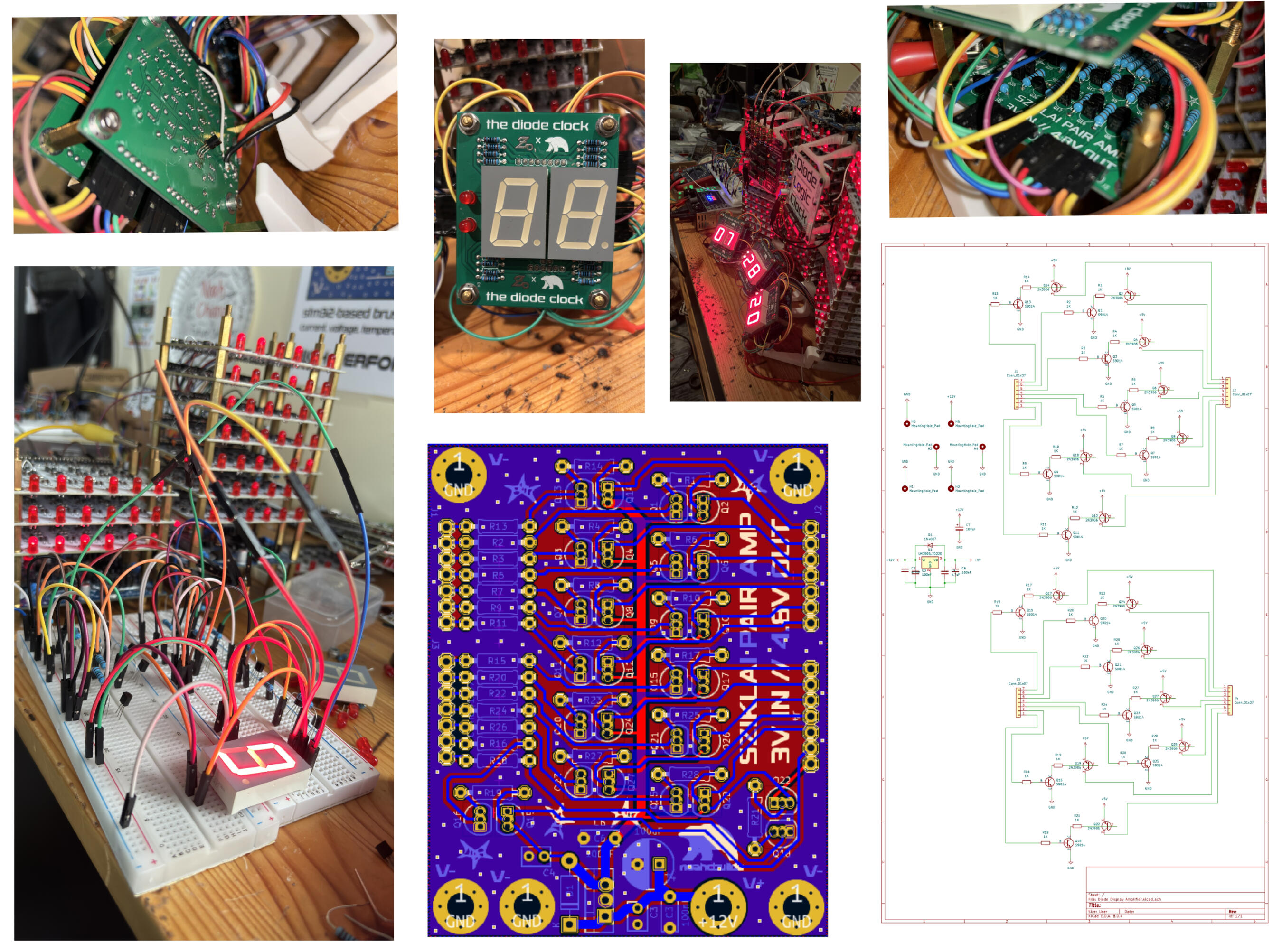
The 7-segment display PCB (top middle) is identical to Yapo's design. However, the LED display Yapo used, the SC10-21SRWA, was modified sometime after 2016. The minimum forward voltage of its segments was increased from 1.8V to 3.7V. The Mouser listing never updated this, and only after testing their operation and closely inspecting the manufacturer's datasheet did I find out.The logic board outputs were still able to make the segments faintly light up. But after seeing how brightly they glowed at saturation, I resorted to using transistors to amplify the display input signals. Sziklai pairs level shift the logic gate output from 3V to 4.8V and provide enough current to fully turn on the displays. They are very pretty, especially at night.The bottom left, middle, and right pictures show the amplifier circuit testing breadboard, PCB layout, and schematic, respectively. The top left and right pictures show the front and back of the amplifier PCB. They stack below the 7-segment display boards.
~January 2026
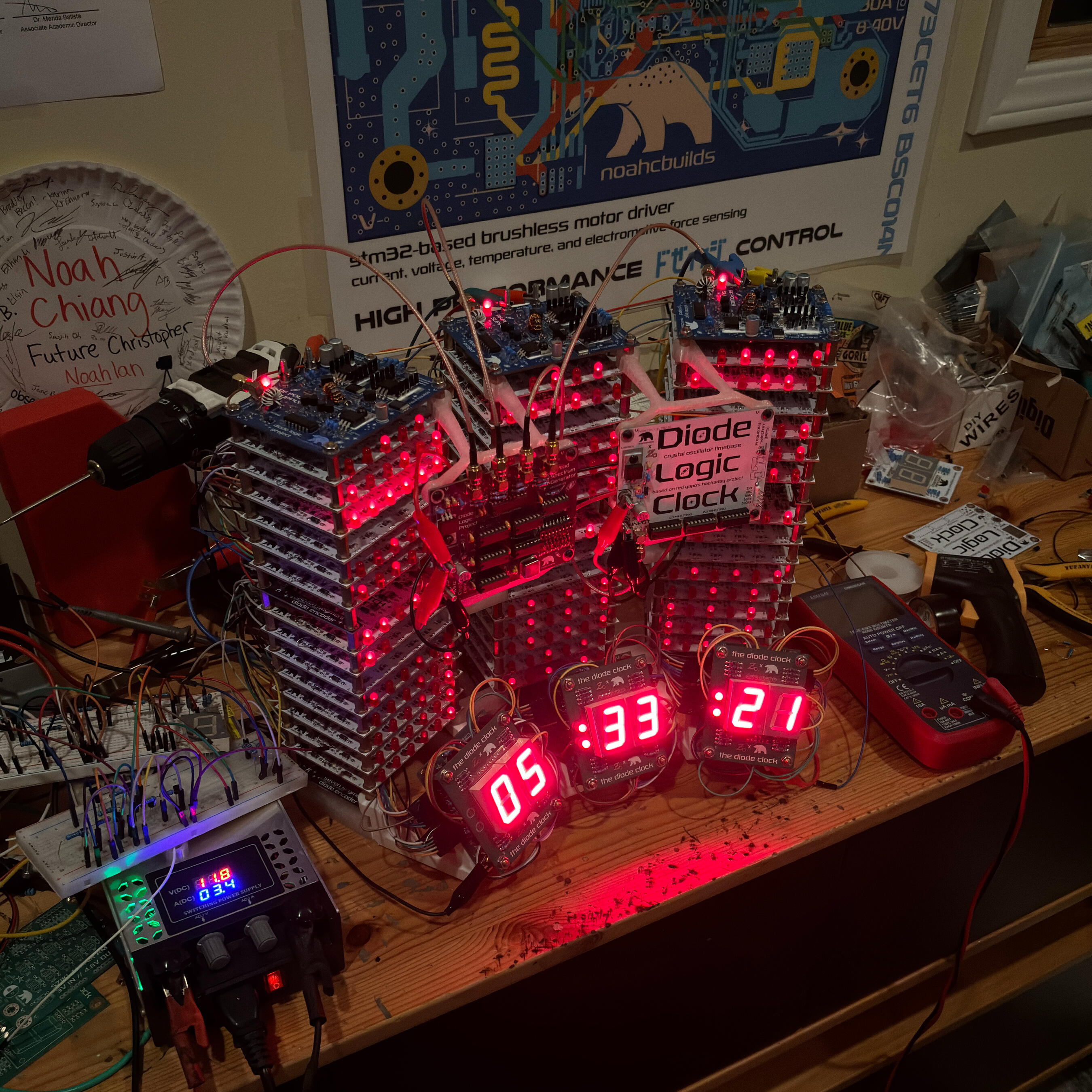
8. Diode Clock Final Assembly
After wiring up all three logic stacks, connecting them in series, and feeding their encoded outputs to the diode amplifiers/displays, the clock was done! My power supply reads 3.5A at 12V (42 watts). Inefficient compared to transistor logic, but much cooler looking. I'll be ready for an overnight test after upgrading the heatsinks on the RF power board's linear regulators. I feel the heat radiating off just by putting my hand nearby!I'm very thankful to Yapo for open-sourcing most of his project, and I'm currently talking with him about putting up a Hackaday post with my board designs and redesigns.
~January to February 2026
300 Hz
Additional photos